
Reverse engineering a keyboard PCB
A few years back, I received a mechanical keyboard from my work – Sentry. It is a beautiful, massive brick of aluminum with a 75% layout. The board came with bluetooth, per-key LED, and key-mappings to switch modifier keys for windows and mac layouts. Initially, the board worked fantastic.
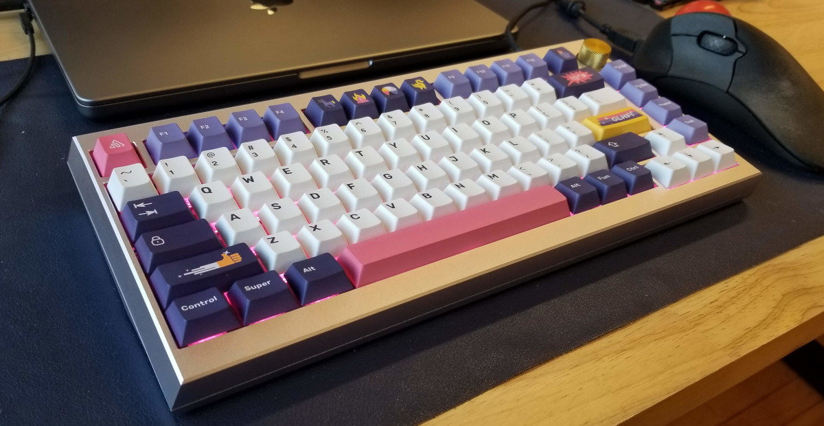
But after 6+ months of having them, I started hearing from my co-workers that their boards were failing. Board failure modes included key chattering, and duplicate character spamming. Some folks were able to repair their boards with newer firmware from the manufacturer. However, many boards stayed effectively broken as you couldn’t reliably type on these devices anymore. While my board was still working, I was worried about its long term health. I was also concerned that the boards at the office would eventually end up in the trash as they failed.
Having worked on several keyboard projects in the past, I wanted to see if I could repair this broken device. After Sentry’s Hackweek was announced in 2026, I decided to try and reverse engineer a physically compatible PCB. My goal was to design and fabricate a PCB that would be a physically compatible replacement. All of the dimensions would be the same, and my PCB would be a true drop in replacement.
Originally the boards had bluetooth, and windows/mac key swapping. To constrain the scope of my project, I would drop a few features and focus on the following:
- Full layout parity. All 82 keys, and the rotary encoder needed to work.
- Per key LED.
- USB-C host port.
- Flashable firmware.
I didn’t want to deal with bluetooth for a few reasons. First, I generally don’t like batteries in devices like keyboards. Second, bluetooth would add significant complexity to the project as it requires additional components for consuming battery power, battery charging, switching between battery and USB power, a radio antenna and a more complex microcontroller that supports bluetooth. Lastly, the keyboard case clocks in at ~4LBs so it is not exactly a ‘portable device’ that would benefit from bluetooth.
Electrical design part 1
The first pass at the electric schematic was pretty simple. I could reuse the schematics for the microcontroller and supporting systems, from a previous build. This project would have a few new components though. First was the rotary encoder, and the second were the SK6812 mini-e LEDS. I had used ‘dumb LEDs’ in a previous build. Dumb LEDs are controlled by an RGB matrix driver that the microcontroller drives over i2c. The SK6812 mini-e LEDs are an addressable device that has a basic binary protocol to encode the red/green/blue values as a stream of bytes. Each LED in the chain consumes one byte per color on each update, forwarding the rest of the data stream to LEDs further down the chain. Addressable LEDs require fewer components, and only require a single rail for data. But are slightly more expensive than dumb LEDs.
Another novel component for this board was the USB connector. Instead of the typical USBc connector, this board would have a picoblade 4 pin jack that connects to the case’s USBc daughter-card.
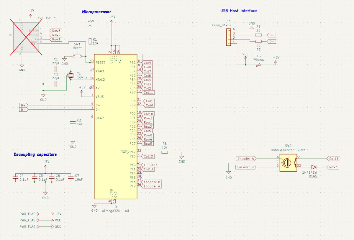
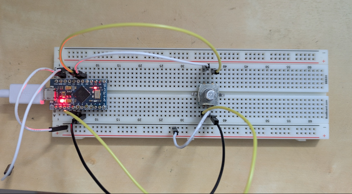
With the basic microcontroller circuitry sorted, I needed to resolve the wiring for the rotary encoder. I had seen a few conflicting examples of rotary encoder schematics in other open source boards. I built a breadboard of the rotary encoder to create a working prototype that I could test with to settle that part of the design.
Physical design part 1
After getting the schematics figured out, the next step was to get the physical layout designed. Because I was aiming to build a physically compatible PCB, I wanted to get the board outline and switches roughly in-place. I started off by disassembling the existing board and measuring it. Using only my trusty art college metal ruler I measured the board outline, and switch landmark locations. These initial measurements would let me place all the components and roughly route the board.
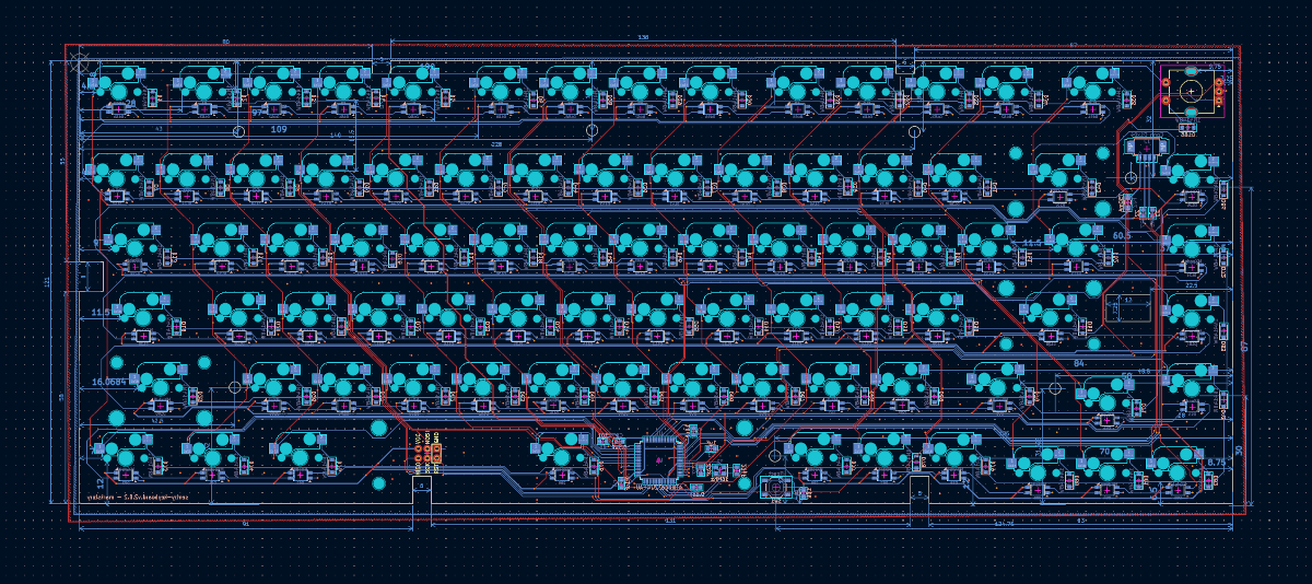
Once I had the board layout roughly figured out, I started using a series of paper prototypes to validate the locations of all the switches with both the existing PCB, and the switch plate.
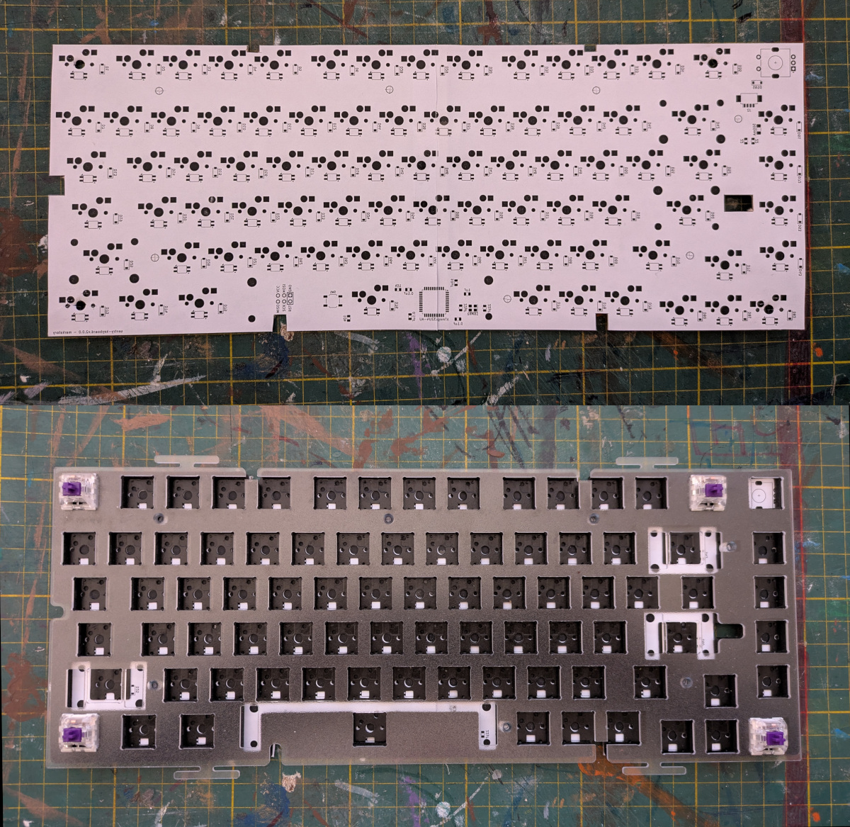
The paper prototypes allowed me to iterate quickly and get most components dialed in. I did several rounds of paper prototyping, and even built some cardboard prototypes to test fit switches, the switch plate and case mounting. Through this process I found several mounting holes were in the wrong place and many switches needed fine tuning to get the placement right.
First board printing
Once I was happy with the paper prototypes, and with Hackweek approaching, I placed an order for PCBs. With the boards in hand, I partially assembled the microcontroller components and host interface. This let me finish developing and testing the firmware, switch matrix and rotary encoder. While the switch matrix worked well, the board was a bit tight in a few places. My metal ruler measurements weren’t accurate enough and I was off by 0.5mm in several places where the PCB fits into the case. The rotary encoder was also off by 0.5mm, and more importantly, the LEDs didn’t work.
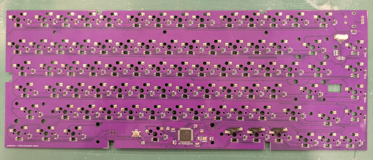
After spending some time with my multi-meter, building a prototype of the LEDs on a breadboard and reviewing the schematic, I tracked the failure back to mistake in the schematics where I had incorrectly wired the VSS and VDD lines on the LEDs.
Better tools and more accurate measurements
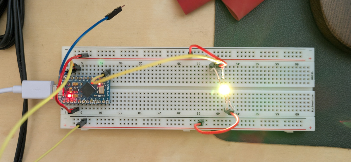
Since the first run of boards had several problems. I would need a second run. I took this opportunity to get a digital caliper so that I could get more accurate measurements for the board shape, switch and encoder placements. A second run would also let me fix the LED schematics. Since I had made a mistake on the LEDs the first time around, I took the time to build a breadboard of the LED wiring to double check my updates.
Second production run
A week after ordering the second batch of boards, I had them in hand. Like last time, I started with the USB host interface, and microcontroller components. I started off soldering a few LEDs on, and tested that they behaved correctly, which they did. Encouraged by the early results of the first few LEDs, I soldered the rest of the 82 LEDs in. When I went to test the full array of LEDs, the board would boot, light up, and ‘crash’ a few seconds later. The ‘crash’ happened as the board cycled through its LED animation and would freeze after a few seconds. I also noticed that the board’s USB interface would disconnect when this happened. Searching on the internet led me to believe that I was dealing with either a short somewhere on the board, a cold solder joint, or a defective LED. My first step was to re-flow and clean up all the LED solder joints. This would help eliminate shorts and cold joint sources of the problem. Sadly, even after re-flowing and cleaning the board the problem persisted. My next theory was that I had a defective LED somewhere, but where? Since all the LEDs are wired in a long chain, I decided to use binary search to try and track down where the problem was. My thinking was that by removing an LED in the middle of the chain and replacing it with a bodge wire I could track down the potentially defective LED more quickly. To my surprise the first halving resulted in a working board!
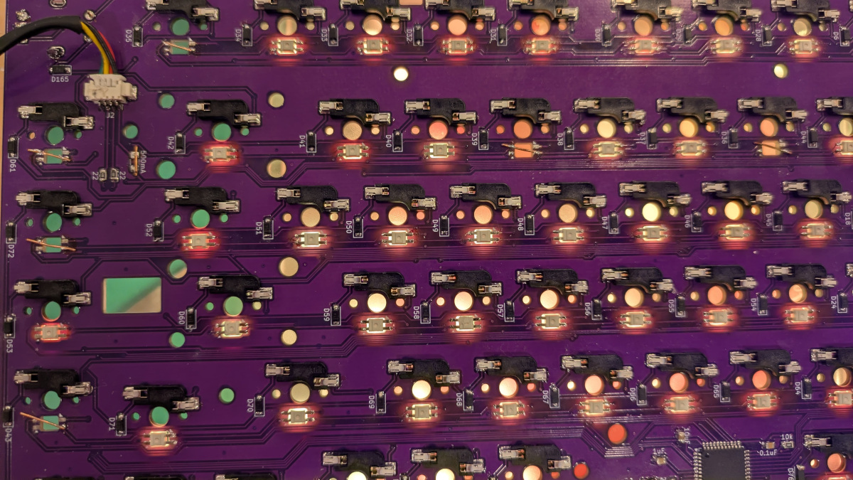
This meant that the problem had to be in the second half of the board! After a few more bisects and bodge wires I was able to narrow down the problem to a small group of LEDs under u,i,o,p. With this sequence, and subsequent LEDs, included the board would crash, but without them the board was fine. What was also strange was that the board would generally crash as the colour cycled to cyan/blue. The fact that crashes happened on cyan/blue and only when the last 15 LEDs were included got me to the root cause.
The root cause ended up being the 500mA fuse. Blue light from an RGB LED draws more power than any other color. With all the LEDs connected, displaying blue was drawing more than 500mA. If I replaced the 500mA fuse with a bodge wire, the board was stable with all the LEDs connected! Once I figured this out, I used my multi-meter to measure how much current the board was using with all the LEDs on, and peak power usage was 1.4A! Almost three times what the USB 2.0 supports. By default QMK sets LEDs to their max brightness – which is blindingly bright. With some more testing I found a brightness level that would only draw 750mA which is above what the USB 2.0 specs support (500mA), but is within the USB 3.0 spec (900mA). Even at the reduced brightness the board was still very bright, and I updated the keymap to include a layer with LED controls so that the animation, brightness and hue could be adjusted later to draw less power if necessary.
Wrapping up
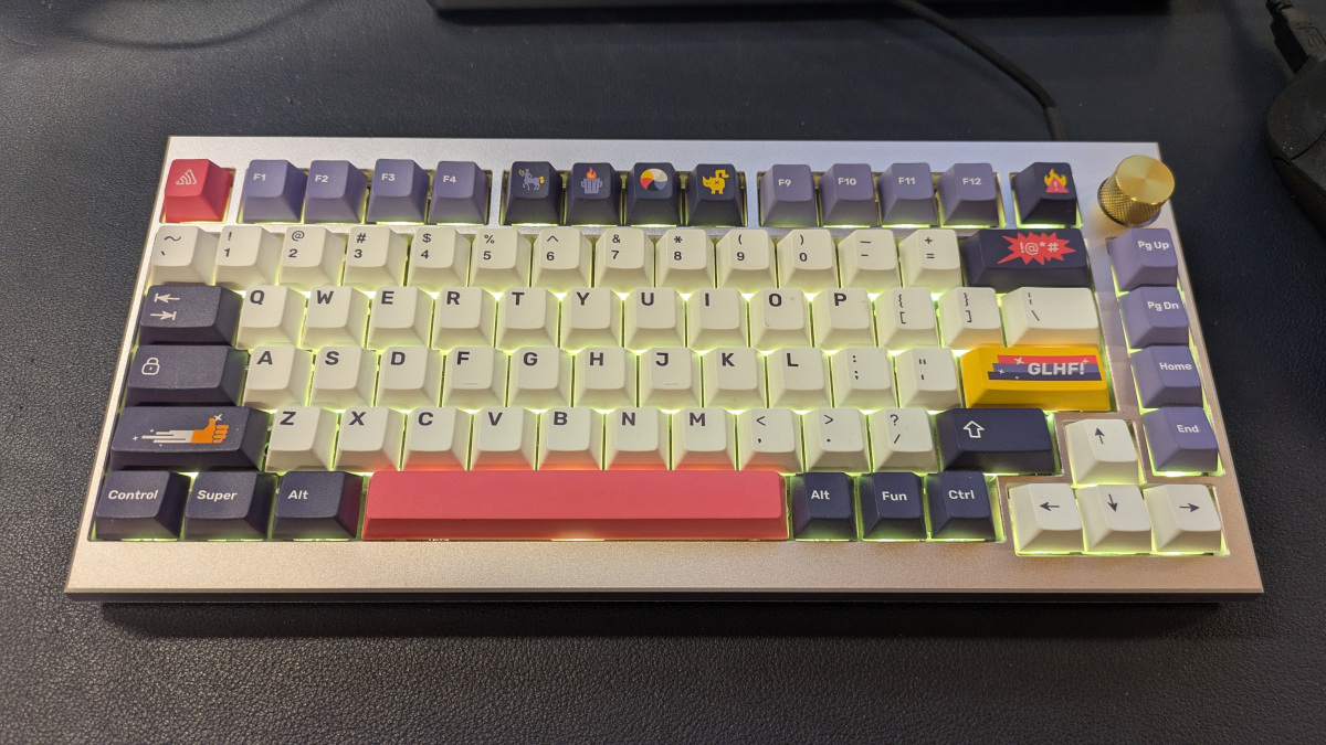
With the LED issues figured out, I was able to successfully repair a keyboard and rescue it from the trash-bin. A couple key takeaways for me were the importance and value of having very accurate measurements. Keyboard tolerances are <0.5mm, so a digital caliper is a must have tool. I should have done the breadboard for LEDs much earlier as it would have caught the wiring issue.
All of the electrical design files, and firmware are available on my GitHub
There are no comments, be the first!